The schematic diagram below shows a simple trivial low-cost 12 volt DC 50W off-line SMPS switching power supply circuit. It can be used for DIY home projects or to learn operation of flyback converters. This PSU can work over a universal input AC line range 90-264 VAC. It provides a nominal 12V DC output at more than 4A load. Line and load regulation is better then 0.5%.
The unit has over current, over temperature and over voltage protections, as well as passive inrush current limiting. Output ripple are approximately 0.2 V peak to peak in the range 0 to 20 MHz. If you need to get lower ripple, you may put an additional output capacitor or an LC filter outside of the feedback loop. This project is a modification of a 24V circuit that I've designed many years ago as a consultant for a small company. That company wanted a plug-in replacement to a cheap off-the-shelf AC to DC power supply, which had a long lead time. By the time I've completed the design and built a proto, they found the off-the-shelf part elsewhere in stock. So, they never proceeded with a manufacturing of this module. Accordingly, I have not tested this design beyond a basic DVT. You can build this circuit for personal use (at your own risk of course). But you are not allowed to republish the content of this page anywhere or use it for commercial purposes without my permission.
SAFETY WARNING.
To safely test or troubleshoot this circuit it is recommended to power it via an isolation transformer or from an isolated AC source. Also note that an offline single-transistor flyback converter generates internal voltages which may reach 600 V. Don't try to play with this circuit unless you are of a legal age, understand power electronics and know how to deal safely with high voltage. You may want to take our quick power supply safety quiz.
CIRCUIT OPERATION.
This AC to DC power supply utilizes a fly back, which is the simplest SMPS converter topology. It uses an 800V/11A MOSFET (Q1) as the switching device and PWM controller UC3844AN (U3). The input section includes a fuse, EMI filter, inrush current limiting NTC resistor R1, a full bridge rectifier CR1, and a DC bus filter capacitor C2.
The initial start-up current for the PWM IC is provided by "bleeding" resistors R7, R8 that allow small current which charges the Vcc capacitor C7.
When the Vcc pin of U3 reaches the positive under voltage lockout threshold (typically 14V-16V), the IC starts to operate and will be driving ON and OFF the switch Q1 via a gate drive resistor R4 at a fixed frequency (in this circuit it is 100 kHz). When Q1 turns on, the DC bus voltage is applied across the transformer T1 primary winding, current through the transformer primary ramps up and energy is accumulated in the transformer's magnetic field. Diodes D4 and D7 during this time interval are reversed biased. When Q1 turns off, the energy stored in the magnetic field causes the voltages across all winding to reverse polarity. As a result, output rectifiers D4 and D7 conduct and the stored energy is transferred to the output and to the bias circuit.Once the converter is started, the bias for the control PWM comes from the bias winding of the transformer.
The secondary side feedback control loop uses a TL431 precision shunt regulator D1 as both the reference and an error amplifier. It compares divided output voltage to D1's internal reference 2.5V. An optocoupler U1 feeds the current proportional to the error signal across the transformer galvanic isolation boundary back to the primary PWM. If accurate regulation of the output is not required, the feedback can be taken from the bias voltage at C9 and fed via a divider into feedback pin 2.
Primary current in T1 is sensed by a resistor R6. This current sense voltage is applied through a spike filter to the current sense terminal of U3, where it is compared against the scaled down error signal at compensation pin 1. When current sense voltage ramp reaches 1/3×(Vpin1-1), the pulse is terminated and Q1 turns off.
Zener diode D6 with optocoupler U2 provide a non-latching output's overvoltage protection.
Thermal switch shuts down the power supply when temperature on the MOSFET heatsink exceeds 95-100 oC.
Here is complete BOM. Note that it was compiled more than ten years ago. Some part numbers may need replacements.
Printed Circuit Boards:
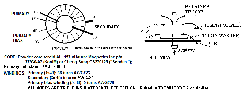
The transformer design may look unusual. Note that a flyback transformer operates as an inductor: it accumulates energy in the magnetic field during ON period of Q1. Then it transfers it (minus losses) into the secondaries during the OFF period of Q1. In order to store energy efficiently with minimal physical size, a non-magnetic gap is needed in series with a high permeability magnetic core material. Flyback transformer design usually uses ferrite cores with a physical gap, or powdered metal cores with an inherently present distributed gap. Gapped ferrites normally feature lower losses, but they have abrupt saturation curve. Powder cores have higher losses, but their B(H) curve is soft. Among other form factors, toroidal transformers have lowest leakage inductance. In this PSU the transformer is made with KoolM powder toroidal core. Proper winding phasing is critical in flybacks just like in all single-ended converters. If windings are misphased the circuit will not work or may simply blow up. Refer to the schematic and winding diagram above for proper transformer installation. All coils in this design have to be made of wire with two or more layers of Teflon insulation to assure reinforced insulation between primary and secondary.


0 comments:
Post a Comment